KEY CONCEPTS
•
Photoelectrochemical water splitting can be used to produce hydrogen and oxygen.
•
Aluminum was able to penetrate through a silicon dioxide layer in a phenomenon known as aluminum spiking to open up pathways for carriers to move through the photoanode.
•
After removal of aluminum through an etching process, nickel was added in an electro- chemical deposition process to catalyze the formation of oxygen.
In moving to a decarbonized economy, the production of green hydrogen is essential. The logical approach is to obtain green hydrogen through efficiently splitting water using renewable energy sources.
But one of the challenges in splitting water is to identify an effective catalyst for the oxygen evolution reaction (OER), which involves the need to transfer four electrons. In contrast, two electrons need to be transferred in the hydrogen evolution reaction which represents a lower energy barrier to overcome.
In a previous TLT article,
1 researchers determined the mechanism for how strontium iridate catalyzes the OER. Surface X-ray scattering and spectroscopic techniques showed that the catalyst changes structure from a crystalline octahedral to an amorphous-octahedron as the reaction proceeds. This shape change is due to the movement of strontium and oxygen ions out of the catalyst and a change in the oxidation state of iridium atoms. The researchers hope that this work will lead to the development of more active OER catalysts.
Another strategy for splitting water is known as photoelectrochemical water splitting. Edward Yu, professor of electrical and computer engineering at the University of Texas in Austin, Texas, says, “We have been studying the use of photoelectrodes in converting water to oxygen and hydrogen. Semiconductors in the photoelectrodes absorb photons from solar energy leading to the formation of mobile charge carriers. Silicon semiconductor absorbers are an appealing option due to their ability to efficiently absorb sunlight. But a key problem is the vulnerability of silicon to corrosion in an aqueous environment.”
But materials that are more stable tend not to be effective in absorbing sunlight. Yu says, “To protect the silicon absorber in a photoelectrode, metal-insulator-semiconductor (MIS) structures have been developed. MIS can be effective, but their thickness prevents charge carriers from tunneling through the insulation stopping the OER.”
Thin MIS structures have been developed, but many are not effective in protecting the photoanode from corrosion caused by the alkaline pH-based environment. Yu and his researchers developed an alternative approach that overcame this problem. He says, “We realized that producing localized conductive paths could facilitate the movement of carriers across even thick insulating layers. However, our original process for preparing the structures needed was complex and time consuming.”
Yu and his colleagues have now devised an alternative approach that uses standard, highly scalable manufacturing processes to establish localized pathways enabling carriers to move across the insulating layer and also enables incorporation of a water splitting catalyst on the photoelectrode surface. They have focused initially on fabrication of photoanodes for OER.
 Evolution of oxygen is facilitated by construction of pathways through silicon microelectronics.
Aluminum spiking
The researchers initially grew 90 nanometer silicon dioxide layers for a MIS photoanode in an oxidation furnace at 950 C under a dry oxygen atmosphere. Then 100 nanometers of aluminum was introduced onto the silicon dioxide surface through the use of DC magnetic sputtering.
Aluminum was then able to penetrate through the silicon dioxide layer via localized pathways that formed when the photoanode was annealed at temperatures between 450 and 600 C. Yu says, “This phenomenon is known as aluminum spiking and is well known in the manufacture of silicon microelectronics. Typically, spiking is undesirable because it leads to short circuits in devices. But, in this case, aluminum penetration through the silicon dioxide opens up pathways for carriers to move through the photoanode.”
The result is that the high resistance initially found with the photoanode steadily declines, with annealing, to 0.5% of its original value.
Yu says, “Aluminum spiking creates pathways for carriers in the photoanode, but, unfortunately, aluminum is not a good catalyst. We, therefore, removed the aluminum by etching in a 10% phosphoric acid solution. The next step was to replace the aluminum with a suitable metal that can catalyze the OER.”
The researchers chose to use nickel and deposited this material using an electrodeposition process. Different applied voltages were used for deposition times ranging from 0 to 120 minutes. Initially, the researchers observed the formation of nickel nano-islands under conditions of low applied voltages and short deposition times. As the applied voltage and deposition time both increased, a continuous nickel film was eventually formed at an applied voltage of -2 V and a deposition time of 120 minutes. Partial coverage of the photoanode by nickel provided the optimal balance between catalytic activity and blocking light from reaching the silicon absorber layer.
The resulting final photoanode structure was placed in an electrochemical workstation (
see Figure 2) that contained a three-electrode electrochemical cell with platinum wire as the counter electrode and a silver/silver chloride reference electrode to evaluate the catalyst’s effectiveness in the OER. The researchers incorporated a p+n-silicon junction to further improve performance. Running the workstation using a standard AM1.5G illumination produced a saturation current density of 32 milliamps per square centimeter. Stability testing run in a one molar potassium hydroxide solution yielded a constant photocurrent density of approximately 22 milliamps per square centimeter over a seven-day operating period.
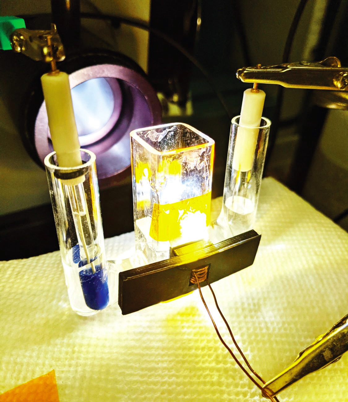 Figure 2. This electrochemical workstation was used to evaluate a photoanode structure produced through an aluminum spiking process. Figure courtesy of the University of Texas.
Yu says, “We believe this approach can be very cost effective and readily scaled up for use commercially. We are now working to develop a similar strategy for the hydrogen evolution reaction (HER), which takes place at the photocathode. Other catalyst materials that are earth abundant and more cost effective than platinum will be explored for the HER reaction.”
Additional information on this research can be found in a recent article
2 or by contacting Yu at
ety@ece.utexas.edu.
REFERENCES
1.
Canter, N. (2021), “Mechanism of water splitting catalyst,” TLT,
77 (4), pp. 16-17. Available
here.
2.
Lee, S., Ji, L., Palma, A. and Yu, Ed. (2021), “Scalable, highly stable Si-based metal-insulator-semiconductor photoanodes for water oxidation fabricated using thin-film reactions and electrodeposition,”
Nature Communications, 12, pp. 1-10.