Mechanism for wear at the atomic scale
Dr. Neil Canter, Contributing Editor | TLT Tech Beat May 2013
Researchers develop a new technique for studying wear.
KEY CONCEPTS
•
A new technique for studying wear at the atomic scales involves using an apparatus similar to an atomic force microscope within a transmission electronic microscope.
•
Using this new technique, researchers evaluated the wear seen when a diamond punch was placed in contact with sharp asperities present at the ends of silicon AFM tips.
•
The wear seen is consistent with a proposed atom-by-atom attrition mechanism and not fracture or plastic deformation.
TWO OF THE CHALLENGES FACING THE LUBRICANT INDUSTRY are minimization of friction and wear. The focus has been to reduce the effect of these parameters at the macroscopic level, for example in the formulation of more advanced automotive engine oils or development of metalworking fluids that enhance the machining of specific metal alloys in particular operations.
Providing a foundation for this effort is work underway to determine the origin of friction and wear at the atomic scale. The key is to determine how atoms present on two interacting surfaces produce friction and wear.
In a previous TLT article, work was reported on an empirical approach about how friction takes place at the atomic scale (
1). Researchers were able to model friction by passing a monolayer of charged polystyrene spheres suspended in water across a light created surface. As the layers passed each other, particles, in some cases, moved closer together to form areas known as kinks, while others moved further apart forming antikink zones. These areas enable particles to move more easily than if all the particles kept the same distance from each other.
To address the mechanism of wear at the atomic scale, STLE-member Robert Carpick, department chair and professor of mechanical engineering and applied mechanics at the University of Pennsylvania in Philadelphia, says, “We currently do not have a good understanding of how wear takes place at the atomic scale. Two processes (plastic deformation and fracture) have been proposed but do not fully explain how wear occurs on the nanometer scale.”
Plastic deformation is characterized by the surfaces changing shape or compressing without any breakage. Fracture represents a large asperity on a surface suddenly breaking off.
Theoretical work has been done that suggests an alternate atom-by-atom mechanism is feasible in which individual atoms from one surface interact with, and are removed by, atoms on a second surface across an interface. Therefore, wear is defined as the rate of atom loss from that surface.
Carpick says, “General reaction-rate theory, which is used to determine the rates of chemical reactions, may also apply to determine the rates of wear at the atomic scale.”
Efforts to show that this atomic attrition process can actually be detected empirically have not been successful until now.
COMBINING AFM WITH TEM
Carpick, in collaboration with STLE-member Tevis Jacobs, a doctoral student in the department of materials science and engineering at the University of Pennsylvania, has developed a new technique for studying wear at the atomic scale that involves using an apparatus similar to an atomic force microscope (AFM) within a transmission electron microscope (TEM).
AFM has been used extensively to study interactions at the atomic scale, but has some limitations in studying wear. Jacobs explains, “AFM is a very sensitive device for examining the atomic scale because it enables us to drag a very sharp tip mounted on a flexible cantilever over a surface, while a laser aimed at the cantilever measures how much the tip moves. But AFM cannot tell what the activity at the tip looks like. While a surface can be detected and wear determined, it is very hard to ascertain the mechanism for wear.”
With TEM, the researchers are able to visualize the wear at the atomic scale. Jacobs says, “TEM enables us to directly image the contact between surfaces. We still cannot see individual atoms, but we can see atomic structure and obtain a picture for how the tip changes over time very accurately.”
Carpick adds, “Use of an AFM probe within a TEM means that we can determine if fracture is occurring, as two surfaces interact with each other through the formation of sharp angles or if plastic deformation is seen by disruptions in the atomic lattice.”
The researchers decided to evaluate the wear seen when a diamond punch was placed in contact with sharp asperities present at the ends of silicon AFM tips. Jacobs says, “The test device was used to observe what happens to the silicon surface as an adhesive force of one nanonewton is applied by the diamond punch during sliding of the surfaces relative to each other.”
Through the use of the TEM, the researchers videotaped each experiment so they could study the interaction between the carbon and silicon surfaces in detail.
Carpick says, “Under the low loads used in this experiment, we observed a gradual, progressive loss of material from the silicon tip, which remained mostly parabolic in shape (
see Figure 1). This is significant because silicon is a brittle material at the macroscale, yet this nanoscale wear was not consistent with brittle fracture.” The result also cannot be explained by plastic deformation. Instead the wear is consistent with the proposed mechanism of atom- by-atom attrition.
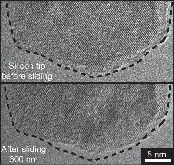 Figure 1. The silicon tip used in evaluating wear is seen before and after sliding across a carbon punch. The gradual, progressive loss of material is consistent with an atom-by-atom attrition mechanism. (Courtesy of the University of Pennsylvania)
Consistent with the results, Carpick speculates that wear occurs by a two-step process. He says, “A silicon atom on the tip forms a bond with one or more carbon atoms on the diamond punch. Then, as the silicon asperity slides on, the bonds that originally held the silicon atom on the tip are broken, leaving the silicon atom behind on the carbon surface. However, there is an energy barrier that needs to be overcome for the initial bond-formation step to occur. Stress applied by the punch lowers the energy barrier, enabling a covalent bond to form between the two atoms.”
Carpick indicates that the sliding speed is a major factor in affecting wear. “All other factors being equal, the more time that the silicon atom is allowed to interact with the carbon atom (or the slower the tip moves) the greater the chance that a bond will be formed,” Carpick says. “This process is analogous to the atoms flirting with each other, and sometimes they decide to get hitched.”
The researchers believe this wear mechanism can easily be dwarfed by more traditional wear mechanisms in macroscopic contacts if large amounts of material are removed. However, Carpick says, “This atom-by-atom mechanism could be applicable to highly polished surfaces sliding for long distances under low loads.”
He adds, “Proper lubrication can minimize contact between the surfaces to prevent this process of atom transfer.”
For the future, the researchers will be evaluating this process at different temperatures and using other materials such as diamond-like carbon, a wear-resistant coating. Additional information can be found in a recent article (
2) or by contacting Carpick at
carpick@seas.upenn.edu.
REFERENCES
1.
Canter, N. (2012), “Observation of Friction on Microscopic Length Scales,” TLT,
68 (4), pp. 8-9.
2.
Jacobs, T. and Carpick, R. (2013), “Nanoscale Wear as a Stress-Assisted Chemical Reaction,”
Nature Nanotechnology,
8 (2), pp. 108-112.
 Neil Canter heads his own consulting company, Chemical Solutions, in Willow Grove, Pa. Ideas for Tech Beat items can be sent to him at neilcanter@comcast.net
.